
Urgent customer's urgency, think what customers want,
Take the quality as the root, service for this
 Order Hotline: Order Hotline: |
| 0755-85298917-606 |
Urgent customer's urgency, think what customers want,
Take the quality as the root, service for this
| Order Hotline: |
| 0755-85298917-606 |

Shenzhen wanchuangxing electronics co. LTD
Contact number:
0755-85298917-606(Sales department)
0755-85298917-602(The Marketing Department)
0755-66802023(Market line)
fax:0755-85298017
e-mail:szwcxpcb@163.com
24H Service telephone:
18028766818(Mr. Wu)
15999646351(Ms. Wu)
URL:Http://www.wcxpcb.com
address:Building 5, fuyong tong tailli industrial park, baoan district, shenzhen
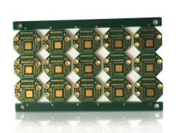
Blind burial production
Now multi-layer board is generally made of a number of two-layer board, and only through the hole of the board as long as a few pieces of two layers directly to the punch and then punch can be very simple (pay attention to copy the thickness and aperture The size of the hole design: When the depth of the hole more than 6 times the diameter of the hole, you can not guarantee uniform wall copper plating)
There are blind buried hole is more trouble:
Such as an 8-layer board 1-2 3-4 5-6 7-8 (here is 4 2-layer board) There are several processing methods
First, let's take a look at the first order
1, the most simple and most common is the first four of these two layers of spittleboard perforation (that is, blind buried hole), respectively, there are 1-2 7-8 two blind holes and 3-4 5-6 such two Kind of buried hole, and then put the four two layers together with the punch and then punch, there are 1-8 of the hole, and this is only once, the production is simple, the cost of comparison at the end.
Due to the different requirements of the PCB stack, the distribution of the wiring layer, the grounding and the power supply layer is different, the first processing method can not meet the PCB design needs, so we want to change the design and production.
Here we look at how to do the second order
2, (1-2 + 3-4) + (5-6 +7-8) Here first of all have to put the four two layers of drilling (that is, blind buried hole), respectively, 1-2 7 -8 such two blind holes and 3-4 5-6 such two kinds of buried hole, and then (1-2 + 3-4) pressed punch, there are 1-4 blind holes, and then 5 -6 +7-8) punching punch, there is a 5-8 blind hole, and then the two four-layer board pressure hole, there are 1-8 of the hole, and although more Two holes, but pressed twice, the production is more complex, high rate of bad, very few factories are willing to do
3, (1-2 + 3-4 +5-6) +7-8 or 1-2 + (3-4 +5-6 +7-8) I will not say
Some people think that I only play one or a few blind buried holes, not expensive to go there? But in fact due to the complete change in the mode of production, the cost and playing a lot of blind buried holes almost.
Some people design blind burial hole on the top of the 8-layer example, he designed the 1-6 and 3-8 holes, how do you design the factory how to press? Do 1-6 can not do the hole of the 3-8, ah, there are some people more excessive, but also the design of 1-3 and 5-7 such holes, how do you want to plant processing? With 3 layers and 1 layer board pressure?
I believe we should be helpful
In the protel99se, press O + K in the lower right corner there is a Drill Pairs button, you can set the hole inside the pair, so that when you line for the time to meet the inside of the hole on the set, the software will Automatically help you add that blind buried hole
In powerpcb or pad, set -> rig on ...
In allegro, set up? Vias? Define B / B through
Can also be kept in the pad, and then added to the PCB
set up ? The constraint...? Physical (line / through) rule set Set the value
When the line in the right side of the option to add (open which two layers will automatically elected through)


 wangwang